Designing Fixtures in PCB Assembly
Printed circuit board (PCB) assembly requires precise, consistent, and efficient operation. Recent technology advancements have reshaped the field of PCB assembly, elevating precision and repeatability as core pillars of manufacturing practices.
In addition to optimizing design parameters, fixture selection is essential for ensuring the best possible outcome. The right pcb printed circuit board assembly test fixture can significantly enhance production efficiency, reduce manufacturing costs, and ensure that product quality is consistently high. A quality test fixture should have an optimized electromechanical interface, mounting hardware, frame/enclosure, and UUT handling mechanism tailored to a specific application. Careful fixture design considering factors like test access, signal integrity, probe density, contact force, thermal management, longevity, and breeding provisions for design changes ensures that the testing process delivers on its potential benefits.
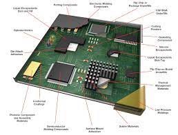
PCBs are the essential building blocks of modern electronic devices and industrial controls. They feature a conductive layer with copper traces that facilitate communications between components and enable electrical current to flow through the circuit. The conductive layer is created through etching, in which a chemical solution dissolves portions of the copper to create the desired traces. Modern PCBs often employ surface-mount technology to minimize the size and cost of the finished product.
Key Considerations for Designing Fixtures in PCB Assembly
During the assembly and inspection processes, PCBs must be carefully evaluated for defects. For the best results, a combination of a boundary scan, automated ICT test points, X-ray laminography, and visual inspection is the ideal approach. This allows the CM to detect and address issues such as missing solder mask, component alignment, and shadowing between pads.
The success of a PCB assembly project hinges on many factors, including the correct placement and orientation of the board’s components. The smallest errors can make a big difference in determining whether a finished product will function properly or experience immediate failure. Incorrect component placement can also drive up costs, which should be a primary consideration for PCB manufacturers.
Another important consideration is the correct choice of soldering materials. Manufacturers should choose lead-free alternatives that meet industry standards without compromising performance and reliability. They should also consider the design of the substrate, as closely coupled planes can help reduce impedance discontinuities and excessive electromagnetic radiation.
Printed Circuit Board (PCB) assembly is a critical process in electronics manufacturing, where individual electronic components are soldered onto a bare PCB to create a functional electronic device. This process encompasses various stages, from component placement to soldering and testing, ensuring the final product meets quality standards and functional requirements.
At the heart of PCB assembly is the PCB itself, which serves as the foundation for all electronic components. PCBs are typically made of non-conductive substrate materials, such as fiberglass or epoxy resin, with copper traces etched onto their surface to create electrical pathways. These pathways connect the various components, allowing them to communicate and function as a cohesive unit.
It’s crucial for PCB assembly manufacturers to prioritize compliance with industry norms and regulations as part of their operational ethos. Doing so enables them to deliver products that consistently meet rigorous performance criteria and fosters trust among consumers, partners, and regulatory bodies. Additionally, adherence to these standards helps ensure that the manufacturer’s products are safe for use and contribute positively to environmental sustainability.